Introduction to Scientific InGaAs FPA Cameras
Overview
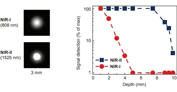
Working in the near infrared (NIR) and shortwave infrared (SWIR) regions of the spectrum offers researchers several advantages, such as the abilities to circumvent unwanted fluorescence backgrounds and to probe more deeply into sample surfaces .
Imaging and spectroscopy techniques performed in the NIR/SWIR are playing an increasingly important role in many leading-edge scientific and industrial endeavors, including the latest R&D efforts to improve solar cells , nanotubes , and semiconductors , as well as studies involving multispectral investigation . The recent introduction of deep-cooled camera systems that employ indium gallium arsenide (InGaAs) focal plane arrays (FPAs) promises to both amplify and broaden the utility of NIR/SWIR imaging and spectroscopy.
Even though light in the NIR and SWIR regions is invisible to the naked eye, its properties are quite similar to those of light in the visible (VIS) region of the spectrum. Like VIS light, NIR/SWIR light is reflective and can provide fine contrast and resolution in images acquired with an appropriately sensitive detector (e.g., an InGaAs FPA). This technical note offers an overview of InGaAs FPAs and discusses key performance features of InGaAs-based cameras for lowlight scientific imaging and spectroscopy applications in the NIR/SWIR regions of the spectrum.
InGaAs FPA Basics
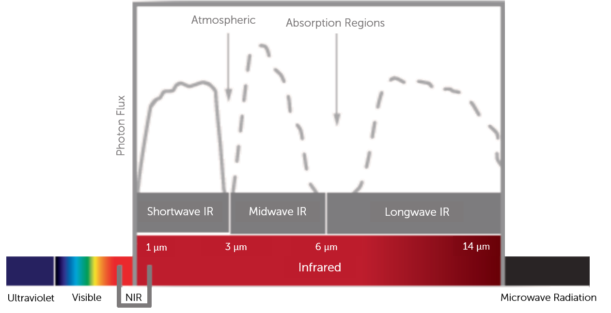
InGaAs is a III-V compound semiconductor that provides excellent photosensitivity in the NIR/SWIR (see Figure 1). Changing the doping concentration of InGaAs alters its sensitivity, thus enabling the spectral response characteristics of the material to be tailored to best meet specific application requirements.
An InGaAs FPA consists of a two-dimensional photodiode array (PDA) — itself comprising an indium phosphide (InP) substrate, an InGaAs absorption layer, and an ultrathin InP cap — that has been indium bump bonded to a readout integrated circuit (ROIC), as shown in Figure 2. State-of-the-art Teledyne Princeton Instruments' NIRvana family of cameras, for example, feature a two-dimensional 640 x 512 array bonded to a low-noise ROIC.

ultrathin InP cap) indium bump bonded to a readout integrated circuit.
In an InGaAs FPA, the two-dimensional array detects incident light and then generates and collects charge; the ROIC clocks and converts the collected charge to voltage and transfers the resultant signal to off-chip electronics. InGaAs FPAs are typically back illuminated and are typically sensitive over the 900 - 1700 nm wavelength range (Figure 3).
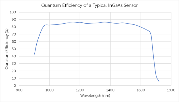
Figure 3: The QR of a standard InGaAs FPA at room temperature.
InGaAs FPA vs Si-CCD Cameras
Currently, many life and physical science applications use low-light-level CCD (silicon-based) cameras for optical imaging and spectroscopy. Although these Si-CCD cameras provide excellent QE in the UV-to-NIR range due to silicon's bandgap properties, even the best NIR-optimized CCDs cannot offer sensitivity beyond 1100 nm (see Figure 4).
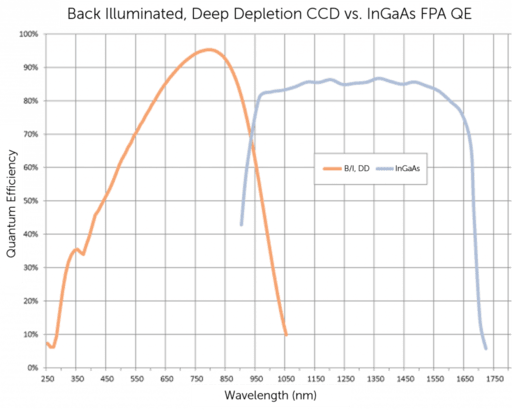
Figure 4: Back-illuminated, deep-depletion silicon CCDs improve sensitivity in the NIR. A thicker, higher-resistivity
epitaxial layer allows these devices' potential wells to penetrate more deeply into the silicon so as to increase
QE at longer wavelengths. Nonetheless, InGaAs FPAs provide better QE above 900 nm.
For over a decade, back-illuminated, deep-depletion silicon CCD cameras have been a preferred tool for NIR imaging and spectroscopy due to their high resolution , relatively inexpensive cost , and acceptable - albeit less than ideal - QE in this region of the spectrum.
New InGaAs FPA cameras, however, extend application utility well into the SWIR (see Table 1). While InGaAs provides sensitivity over an extended NIR range due to its lower bandgap . The lower bandgap is also responsible for much higher dark current (thermally generated signal) compared to Si-CCDs. As a result, scientific InGaAs FPA cameras require very deep cooling (i.e., down to -85°C) to minimize this unwanted noise source.
| Specifications | InGaAs FPA | Si-CCD |
| Typical Pixel Size | 20 μm2 | <8 μm2 to > 24 μm2 |
| Typical Resolution | <640 x 512 | 512 x 512 to >2k x 2k |
| Wavelength Response (nm) | 900 - 1700 | <200 - 1100 |
| Typical Dark Current (e-/pixel/sec) | 300 (incl. ambient background) | 0.0001 |
| Fixed Pattern Noise | Present | Low |
Scientific InGaAs FPA Camera Performance
Commercial NIR cameras incorporating InGaAs FPA sensors are typically designed for use in night vision and thermal inspection applications . Scientific applications, on the other hand, impose extreme demands on camera systems to achieve the best possible signal-to-noise ratio (SNR) . This section discusses the key performance features of scientific InGaAs FPA cameras.
Sensitivity/Quantum Efficiency
As discussed above, typical InGaAs FPAs have sensitivity between 900 and 1700 nm. However, great care must be taken to maximize photon collection before the incident light reaches the sensor. For example, it is important to use a single optical window in the camera, treated with an antireflective coating (AR coating) to maximize photon throughput.
One of the particularly noteworthy behaviors of InGaAs FPAs is that their long-wavelength cutoff is reduced when they are cooled . As a rule of thumb, the long-wavelength cutoff shifts by 8 nm for every 10°C of sensor cooling. This phenomenon can actually be advantageous, as the sensor is insensitive to background signal beyond the shifted far-end wavelength cutoff. In other words, the sensor acts like a "tunable" lowpass optical filter (see Figure 5).
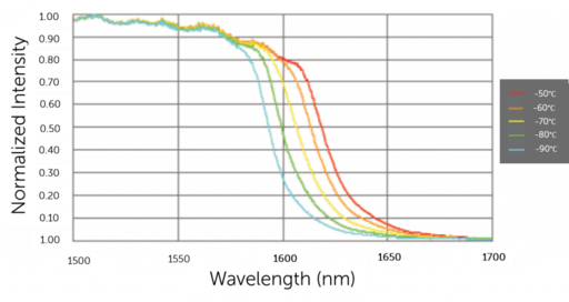
Figure 5: The far-end wavelength cutoff of InGaAs shifts twards blue with device cooling.
The typical shift is about 8 nm per 10°C.
Dark Noise
InGaAs FPAs are dark-noise-limited devices . Deep cooling, down to -85°C, is required to reduce dark charge (see Figure 6) and preserve the signal-to-noise ratios needed for scientific applications. Refer to "The need for cooling" below.
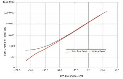
Figure 6: Deep cooling greatly reduces dark charge for InGaAs FPAs.Total dark charge (sensor dark current +
ambient dark current) is shown. The difference in the measured dark charge of the FPA at low temperatures
using a Room Temp Target versus an LN Temp Target is attributable to the atmosphere between the window
and the target, as well as heat detected from the Room Temp Target.
Using a deep-cooled InGaAs FPA camera, continuous exposure times of several minutes are practical (see Figure 7).
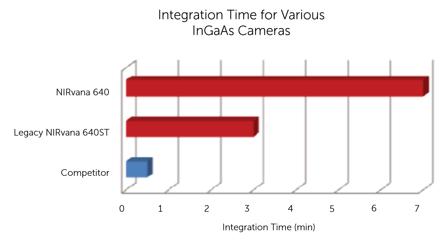
Figure 7: Deep-cooled InGaAs FPA cameras enable the use of longer continuous exposure times.
Pixel Defects
Due to a very complex manufacturing process, almost every InGaAs FPA has a small percentage of defective pixels - non-uniform, dark, and bright. A non-uniform pixel demonstrates greater or lesser photosensitive response than the surrounding pixels (i.e., its response, though linear, differs from the average response demonstrated by the rest of the device's array). A dark pixel , meanwhile, is unresponsive to light and appears black in an image. Finally, a bright pixel is a pixel that saturates independently of incident light and appears as a white spot in an image (see Figure 8).
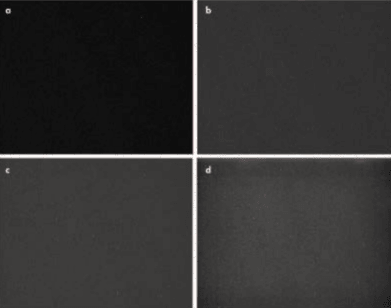
Figure 8: The occurance of bright pixels increases as exposure time increases: (a) 1 msec, (b) 1 sec,
(c) 10 sec, and (d) 60 sec. Images acquired with a deep-cooled Teledyne Princeton Instruments
NIRvana:640 InGaAs FPA camera system.
While pixel defects are inevitable when dealing with InGaAs FPA devices, it is desirable to have a defect-correction algorithm built into the camera's acquisition software or hardware for scientific applications. LightField™ software from Teledyne Princeton Instruments, for example, provides automatic pixel defect correction for defects up to 2 x 2 pixels in size.
Fixed pattern noise
In addition to the aforementioned pixel defects, InGaAs FPA camera system users should be aware of one more performance characteristic of these devices. In a typical InGaAs FPA, each pixel (or pixel column) is connected to an individual preamplifier for readout, so any gain/response variations will cause fixed pattern noise (FPN). In advanced cameras such as the NIRvana:640, the FPN is fully subtractable (see Figure 9).
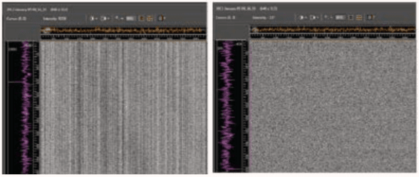
Figure 9: Advanced cameras, such as the NIRvana, is able to fully subtract fixed pattern noise within software.
The Need for Cooling
Due to the low bandgap of InGaAs material, InGaAs FPA cameras have much higher dark current than Si-CCD cameras. Therefore, it is absolutely critical to minimize InGaAs FPA cameras' dark noise via deep cooling . Scientific InGaAs FPA cameras, for example the NIRvana:640 use advanced thermoelectric cooling and vacuum technology to cool sensors down to -85°C and achieve the lowest possible dark noise.
The NIRvana family of cameras uses an all-metal, hermetically vacuum-sealed chamber (see Figure 10) with a single vacuum window for maintenance-free operation:
• State-of-the-art design cools sensor down to either -85°C or -65°C.
• Single optical window with double-sided AR coating provides the highest photon throughput , >98% transmission, in the NIR band.
• Hermetic seals afford maintenance-free operation . No vacuum re-pumping is necessary over the camera system's long lifetime.
• High vacuum levels deliver deep sensor cooling and condensation-free operation.
• Built-in air or liquid cooling options allow researchers to utilize a built-in fan for optimal ease of use or an external liquid circulator for vibration-free operation (the built-in fan can be turned off via software).
• A proprietary cold-shield minimizes the detection of unwanted ambient NIR radiation . The cold-shield is a metal component that sits on top of the InGaAs FPA and is cooled to the same temperature as the sensor. It limits the f-cone of the sensor (typically f/1.5) and reduces background for lower overall noise.
• Cooling shifts the long-wavelength cutoff by about 8 nm for every 10°C, thus reducing unwanted background noise .
Conclusion
Newly available scientific, deep-cooled, large-format InGaAs FPA cameras such as the as the NIRvana family from Teledyne Princeton Instruments (see Figure 11) will enable researchers to work more effectively than ever before at longer wavelengths in the NIR and SWIR regions of the spectrum. Key applications include nanotube fluorescence, emission, absorption, small animal imaging, nondestructive testing, and singlet oxygen detection.

Figure 11: The Teledyne Princeton Instruments NIRvana family of InGaAs FPA cameras, with advanced
thermoelectric cooling or liquid nitrogen cooling options. The camera's state-of-the-art electronics
perform off-chip digitization.
Back-illuminated, deep-depletion silicon CCD cameras such as the Teledyne Princeton Instruments PIXIS:1024BR, meanwhile, continue to offer superb resolution and sufficient quantum efficiency for cost-effective imaging and spectroscopy at shorter NIR wavelengths.
Teledyne Princeton Instruments is the only company that provides both deep-cooled InGaAs FPA and silicon CCD cameras suitable for advanced imaging and spectroscopy applications in the NIR and SWIR.

