InGaAs Cameras: The Basics
InGaAs Sensors
InGaAs sensors are used for applications in physical and life science that require high sensitivity over the 900-1700 nm wavelength range, referred to as shortwave infrared (SWIR). Some InGaAs sensors are able to measure up to 2500 nm due to changes in material composition.
While silicon-based CCD cameras have excellent sensitivity over the UV-to-NIR range, the bandgap properties of silicon prevent these CCDs from having sufficient sensitivity over 1100 nm. However, InGaAs cameras have a lower bandgap, making this material the preferred technology for applications in the shortwave infrared (SWIR) region.
An InGaAs focal plane array is made of a two-dimensional photodiode array. This array consists of an indium phosphide (InP) substrate, an InGaAs absorption layer, and an ultrathin InP cap that has been indium bump bonded to a readout integrated circuit (ROIC). A diagram of this can be seen in Figure 1.
The InGaAs two-dimensional array detects SWIR incident light, by collecting the photon generated charge. The ROIC clocks and converts the collected charge into voltage, transferring the signal to off-chip electronics where it is used to create an image.
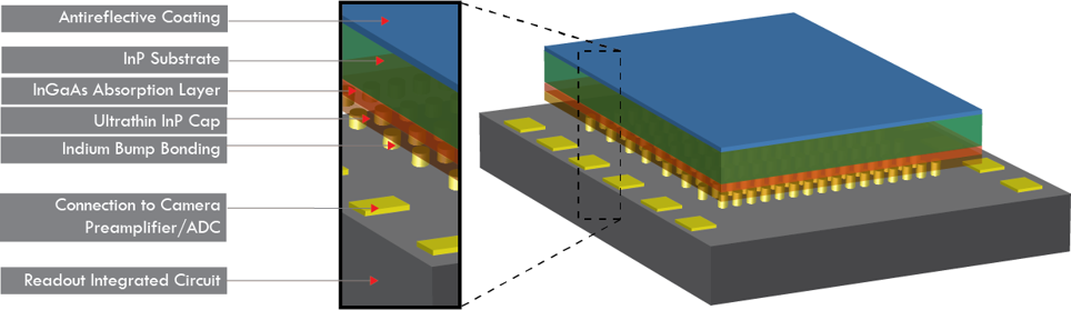
Figure 1: Diagram showing the different layers of a typical InGaAs sensor. The top layer (blue) consists of an antireflective coating to maximize photon throughput. The next layer (green) is the InP substrate, which is connected to an InGaAs absorption layer (orange) underneath, followed by an ultrathin InP cap (yellow). This cap is then indium bump bonded (yellow columns) to the readout integrated circuit (grey) onto which the camera preamplifier (yellow cuboids) connects.
Limitations
The biggest limitation of InGaAs cameras is their noise level. The lower bandgap of the material also produces higher dark current (thermally generated signal). Therefore, InGaAs cameras need to be deeply cooled to increase signal to noise by reducing dark noise as much as possible.
This is achieved either by thermoelectric cooling or by cryogenic cooling dependent on application requirements. The sensor is located in a hermetically vacuum-sealed chamber to ensure low thermal coupling of the sensor to the outside environment and prevent condensation of residual gas on the sensor. The highest quality vacuum chambers offer maintenance free cooling of the camera over their lifetime. Figure 2 shows how dark charge decreases with decreasing temperature.
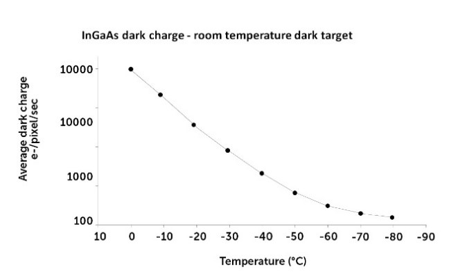
Figure 2: The relationship between dark noise and temperature, indicating a reduction in electrons per pixel per
second with a reduction in temperature.
Another limitation is pixel defects. Due to the intricacy of InGaAs sensor fabrication defective pixels are inevitable, however these can be corrected for using a defect-correction algorithm within the data acquisition software.
Fixed pattern noise is also an issue, caused by gain or response variations. In typical InGaAs focal plane arrays, each pixel column is connected to an individual preamplifier for readout, resulting in a fixed pattern noise from any gain/response variations. However, within advanced InGaAs cameras this is can be fully subtracted.
Summary
InGaAs sensors are optimized for detection in the SWIR range due to their lower bandgap. These sensors are made of a 2D photodiode array comprise of an InP substate, InGaAs absorption layer, and an ultrathin InP cap.
SWIR wavelengths are essential in multiple applications, for examples, within life sciences this wavelength range is easily able to penetrate deeply into in vivo tissue. For industrial applications, InGaAs cameras are essential for humidity measurements, surface film distributions, and the separation of materials; all which rely on photon detection in the SWIR range.
Due to the lower bandgap of the material, InGaAs cameras are susceptible to higher dark noise. This is combatted, however, by deep cooling the camera to reduce the dark noise as much as possible. Another limitation is pixel defects; however this can be corrected for using a defect-correction algorithm within the data acquisition software.
Related Articles
-
 Technology Primer
CCD vs CMOS
Read the Story -
 Tech Note
Camera Resolution
Read the Story -
 Tech Note
ICCD and emICCD Cameras: The Basics
Read the Story